Projects
Zilog Z80,000 | National Semiconductor NS32532 | National Semiconductor NS32764 (Swordfish) | Intel Pentium® Processor (P5) | Intel Itanium Processor (Merced) | Intel 815 Chipset (Solano) | Other Research and Publications
Z80,000 Microprocessor
Zilog
1986
Background
I began working at Zillog in June 1980. I had hoped to get a job designing “real” computers at Amdahl, but they were not hiring. By chance, I had met Ross Freeman, who was Zilog’s Director of R&D, at a Peace Corps event in San Francisco. With Ross’s introduction, I was hired to work for John Banning as an architect of the Z80,000 microprocessor. The Z80,000 was a 32-bit extension to the 16-bit Z8000 that Zilog introduced in 1979. [CHM 2007] Bernard Peuto, who had been the architect for the Z8000, was Zilog’s VP of Engineering at that time.
My work on the Z80,000 was an extraordinary introduction to VLSI technology. I became fascinated by the range of cost, performance, and power tradeoffs for custom circuit design. In particular, I became interested in the tradeoffs among different types of memory (ROM, RAM, CAM) and their relation to computer architecture. This interest followed through to my Ph.D. research. [Alpert 1984] The project was also an opportunity to apply what I had studied at Stanford about mainframes and minicomputers to microprocessors, especially in techniques for instruction pipelines, cache memory, and performance evaluation.
Die Photo

Block Diagram

Key Features
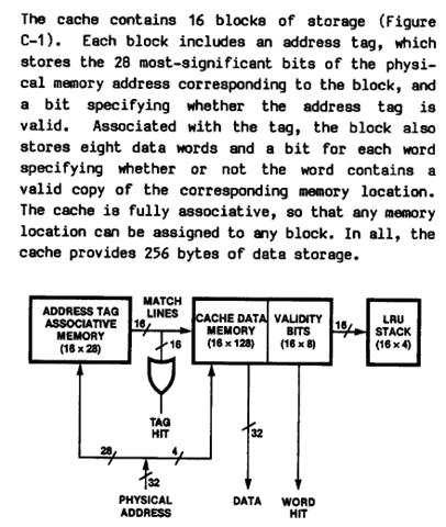
32-Bit Integer Pipeline
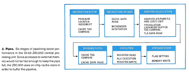
Paged Memory Management
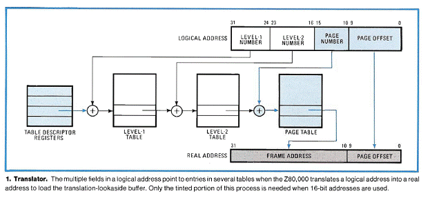
256B Sectored, Unified Instruction/Data Cache
References
[Alpert 1983a] Donald Alpert, “Powerful 32-Bit Micro Includes Memory Management,” Computer Design, October 1983, pp. 213-220.
[Alpert 1983b] Don Alpert, Dean Carberry, Mike Yamamura, et al, “32-Bit Processor Chip Integrates Major System Functions,” Electronics, July 14, 1983, pp. 113-119.
[Alpert 1984] Donald Alpert, “Memory hierarchies for directly executed language microprocessors,” Technical Report 84-260, Computer Systems Laboratory, Stanford University, Stanford, California 94305, June 1984.
[CHM 2007] “Oral History Panel on the Development and Promotion of the Zilog Z8000 Microprocessor,” Computer History Museum, April 27, 2007.
[Zilog 1984] “Z80,000 CPU Preliminary Technical Manual,” September 1984, Zilog, Inc.
NS32532 Microprocessor
National Semiconductor
1987
Background
I joined National Semiconductor’s design center in Herzlia, Israel in May 1985, working for Uri Weiser. NSC had introduced the NS16000 family of microprocessors in 1981, including the NS16032 CPU, NS16082 MMU, and NS16081 FPU to implement a complete 32-bit architecture supporting 32-bit integers, IEEE double-precision floating-point data, and paged memory management. At the time, other merchant semiconductor vendors offered chips that implemented only a subset of these functions. [Bal] Consequently, the NSC architecture was adopted by a number of computer system companies for high-end workstations and minicomputer-class multiprocessors. Unfortunately, the design and validation techniques used by NSC and other chip makers were inadequate to debug a complete computer system.
For the next generation NS32132 CPU NSC had developed much more effective validation techniques to create a very reliable product, but the market opportunity had passed for workstations. The NS32000 line still had design wins for embedded applications, in particular for laser printers that required substantial software to interpret postscript files.
Die Photo

Block Diagram
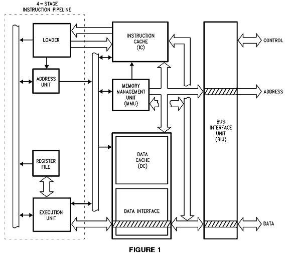
Key Features
Hardware Cache Coherence
The microprocessor’s hardware-based coherence mechanisms include a bus of eight pins that controls total or partial invalidation of the on-chip instruction and data caches. Figure 4 shows the organization of the two-way set-associative data cache and its connection with the invalidation bus. Each of the cache lines within a set has an address tag. 16 bytes of data, and four dual-ported validity bits. Both lines of a data cache set can be invalidated using the invalidation bus. Because the validity bits are dual-ported, invalidation of the on-chip caches occurs without interfering with ongoing cache accesses or bus transactions.
[Maytal, p. 73]
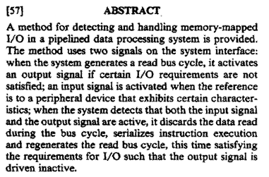
Serialize Memory-Mapped I/O
References
[Bal] S. Bal, A. Kaminker, Y. Lavi, A. Menachem, and Z. Soha. 1982. The NS16000 Family-Advances in Architecture and Hardware. Computer 15, 6 (June 1982), 58-67. DOI=10.1109/MC.1982.1654051 http://dx.doi.org/10.1109/MC.1982.1654051
[Maytal] Benjamin Maytal, Sorin Iacobovici, Donald Alpert, et al, “Design Considerations for a General-Purpose Microprocessor,” Computer, January 1989, pp. 66-76. http://dx.doi.org/10.1109/2.19824
[Alpert ICCD] D. Alpert, J. Levy, and B. Maytal, “Architecture of the NS32532 Microprocessor,” Proceedings ICCD, October 1987, pp. 168-172.
[Alpert CompEuro] D. Alpert, D. Biran, L. Epstein, et al, “Trends in VLSI Microprocessor Design,” Proceedings, First Annual Conference on Computer Technology, Systems and Applications (CompEuro ’87), May 1987, pp. 564-567.
[NS32532DS] NS32532-20/NS32532-25/NS32532-30 High-Performance 32-Bit Microprocessor Datasheet, National Semiconductor Corporation, May 1991.
U.S. Patent 4,802,085, Apparatus and method for detecting and handling memory-mapped I/O by a pipelined microprocessor.
[CHM 2008] “National Semiconductor 32000 Microprocessor Oral History Panel,” Computer History Museum, February 26, 2008. http://archive.computerhistory.org/resources/access/text/Oral_History/102658246.05.01.acc.pdf
Swordfish Microprocessor
National Semiconductor
1991
Background
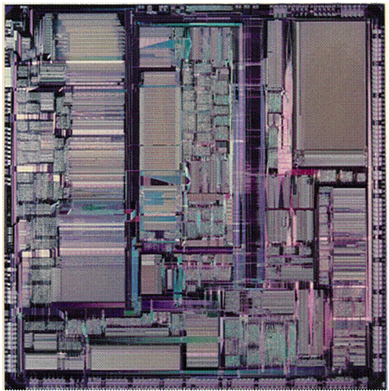
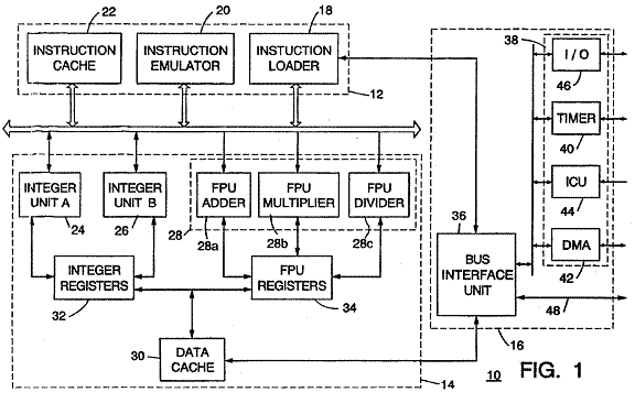
The Swordfish microprocessor was developed to meet the requirements of NSC’s workstation and server customers, as well as for laser printers and other embedded applications. These sometimes conflicting objectives were met by implementing a stripped-down subset of the NS32000 architecture directly in hardware and emulating more complex operations with an on-chip ROM. The result was a single-chip microprocessor that was possibly the first to integrate superscalar integer pipelines, pipelined double-precision floating point pipeline, memory management, and cache. The analysis that went into the design decisions led to master’s theses by Ori Danieli and Giddy Intrater. [Danieli 1990, Intrater 1994]
Die Photo
Block Diagram
Key Features
Superscalar Execution
We were trying to figure out how to get parallelism out of multiple functional units, and adopted a microarchitecture that was like VLIW: each FU [Functional Unit] was assigned to fixed slots in a 2-wide instruction word fetched from the cache. We had the HW detect dependencies as instructions were placed in the cache slots, so it was a superscalar architecture with a VLIW machine organization. To improve icache efficiency we allowed dependent instructions to be packed together with a bit per pair of instructions that indicated whether or not they were dependent. Independent instructions could be executed in parallel, dependent instructions had to be executed sequentially, but still on the pipeline assigned to that slot. Just about the only wasted cache slots were for FP instructions that could not be paired with a load or integer op.
… Overall it was a very efficient architecture. With little extra cost for a second integer pipe and a simple control structure, it was possible to derive a lot of parallelism on many embedded loops.
[Smotherman Swordfish]
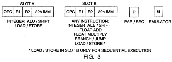
As shown in FIG. 3, each instruction cache entry includes two slots, i.e. Slot A and Slot B. Thus, each entry can contain one or two partially-decoded instructions that are represented with fixed fields for opcode (Opc), source and destination register numbers (R1 and R2, respectively), and immediate values (32b IMM). The entry also includes auxiliary information used to control the sequence of instruction execution, including a bit P that indicates whether the entry contains two consecutive instructions that can be executed in parallel and a bit G that indicates whether the entry is for a complex instruction that is emulated, and additional information representing the length of the instruction(s) in a form that allows fast calculation of the next instruction’s address.
[U.S. Patent 5,481,751, Fig. 3, 6:1-14]
Decoded Instruction Cache

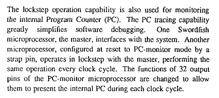
Debugging Support
References
[Danieli 1990] D. Alpert, A. Averbuch, and O. Danieli. “Performance comparison of load/store and symmetric instruction set architectures.” in Proceedings of the 17th annual international symposium on Computer Architecture (ISCA ’90). ACM, New York, NY, USA, 172-181. http://doi.acm.org/10.1145/325164.325137
[Talmudi 1991] Ran Talmudi, et al., “A 100MIPS, 64b superscalar microprocessor with DSP enhancements,” IEEE Intl. Solid-State Circuits Conference, San Francisco, Feb. 1991, pp. 100-101. http://dx.doi.org/10.1109/ISSCC.1991.689081
[Intrater 1991] Intrater, G.; Talmudi, R.; , “A superscalar microprocessor,” Electrical and Electronics Engineers in Israel, 1991. Proceedings., 17th Convention of , vol., no., pp.267-270, 5-7 Mar 1991. http://dx.doi.org/10.1109/EEIS.1991.217646
[Intrater 1994] G. D. Intrater and I. Y. Spillinger. 1994. Performance Evaluation of a Decoded Instruction Cache for Variable Instruction Length Computers. IEEE Trans. Comput. 43, 10 (October 1994), http://dx.doi.org/10.1109/12.324540
Swordfish Microprocessor Architecture Specification, Revision 2.0, February 1990. Appears as Appendix A to U.S. Patent 5,249,286.
[Smotherman Swordfish] http://www.cs.clemson.edu/~mark/swordfish.html
[CHM 2008] “National Semiconductor 32000 Microprocessor Oral History Panel,” Computer History Museum, February 26, 2008. http://archive.computerhistory.org/resources/access/text/Oral_History/102658246.05.01.acc.pdf
U.S. Patent 5,249,286, Selectively locking memory locations within a microprocessor’s on-chip cache
U.S. Patent 5,481,751, Apparatus and method for storing partially-decoded instructions in the instruction cache of a CPU having multiple execution units
U.S. Patent 5,669,011, Partially decoded instruction cache
Intel Pentium® Processor (P5)
1993
Background
After my experience designing three microprocessors in the 1980’s, I was satisfied that the designs had received some technical recognition, but disappointed that none of the hard work had led to commercial success. With NSC I had the opportunity to visit a number of computer system companies to promote the Swordfish product during its development. What I heard consistently was that they liked the technology of maintaining architecture compatibility while using semiconductor improvements to deliver high performance. The system vendors were frustrated that both Intel (with the x86 and 860 product lines) and Motorola (with the 68k and 88K product lines) were forcing their customers to choose between CISC compatibility and higher-performance RISC architectures. They told me that if they had to choose a new architecture, the most important criterion was the installed base of application software. I listened, and I knew that the IBM PC had given Intel’s x86 architecture a growing lead lead in application software, so in January 1989, I took the opportunity to join Intel as the first engineer working on what became the P5 project to develop the first Pentium microprocessor product.
At that time, Intel was only a month away from completing the 486 design. which could execute basic integer instructions with 1-clock throughput and double-precision floating-point instructions in about 20 clocks. Several areas were identified to improve performance for the next microprocessor, including opportunities for certain techniques addressed specifically at limitations of the x86 architecture compared with the newer RISC architectures.
- The x86 architecture had byte-variable instructions, so additional information was stored in the instruction cache to identify instruction boundaries.
- The 486 took 3 clocks for a taken branch, and this could be reduced with hardware branch prediction
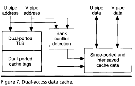
- The x86 had only about 8 general-purpose registers, so there were relatively more memory references than for RISC processors. The P5 used a dual-ported data cache to execute two memory references simultaneously in a single clock.
- The x86 floating-point architecture has no general-purpose registers, using a stack instead. The stack introduced false dependencies between instructions, which limited the overlapped execution of independent instructions. The P5 pipeline could execute an instruction to exchange the top-of-stack with another stack element, which allowed these false dependencies to be overcome to execute independent floating-point operations with 1-clock throughput.
The Pentium microprocessor turned out to be wildly successful, despite the presence of a subtle flaw in the floating-point division operation that caused Intel to write off $500M for the first year’s production. The 5-year business plan for the P5 written in 1990 called for 3M units to be sold in 1995, but the actual amount was almost 30M units, about 10x higher than planned.
Here is a copy of the first hand-drawn sketch of a block diagram from mid-1989, which I prepared for a planning presentation. During the mid-1990’s the original was on display at an exhibit in the Intel Museum to show the very beginning, conceptual stage of the design and manufacturing process for a microprocessor.
Die Photo
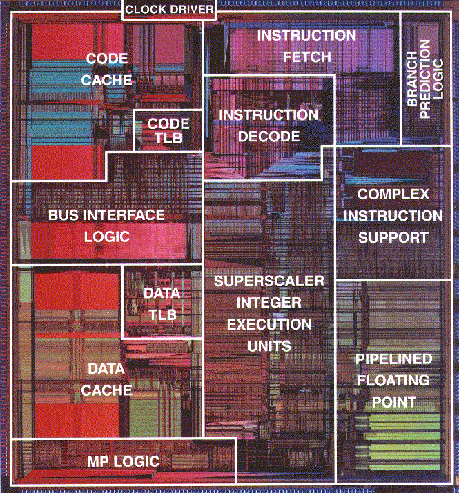
[Alpert 1993, photo from http://bwrc.eecs.berkeley.edu/cic/die_photos/pentium.gif]
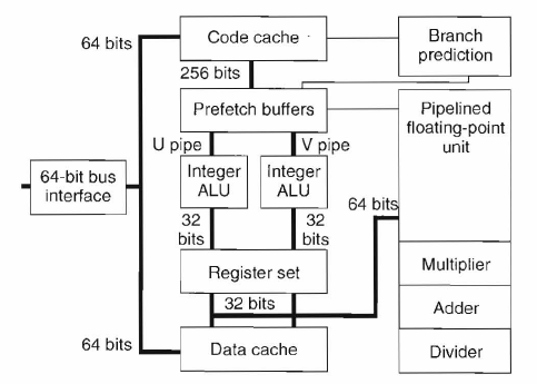
Block Diagram
Key Features
Superscalar Integer Pipelines

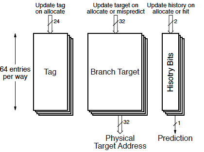
Branch Prediction
Dual-Ported Data Cache
Pipelined Floating-Point Unit

References
[Alpert 1993] Donald Alpert and Dror Avnon, “Architecture of the Pentium Microprocessor,” IEEE Micro 13, 3 (May 1993), 11-21. http://dx.doi.org/10.1109/40.216745
[Case 1993] Brian Case, “Intel Reveals Pentium Implementation Details,” Microprocessor Report, Vol. 7, No. 4, March 29, 1993.
Intel’s Pentium Processor, a lecture by John Crawford, Donald Alpert and Beatrice Fu, https://www.youtube.com/watch?v=dH1fo7jAFnc
U.S. Patent 5,442,756, Branch prediction and resolution apparatus for a superscalar computer processor
U.S. Patent 5,450,605, Boundary markers for indicating the boundary of a variable length instruction to facilitate parallel processing of sequential instructions
U.S. Patent 5,475,824, Microprocessor With Apparatus For Parallel Execution Of Instructions
U.S. Patent 5,479,652, Microprocessor with an external command mode for diagnosis and debugging
U.S. Patent 5,559,986, Interleaved cache for multiple accesses per clock cycle in a microprocessor
U.S. Patent 5,657,253, Apparatus for monitoring the performance of a microprocessor
Intel Itanium Processor (Merced)
It was nearly 10 years ago that Lew Platt first contacted Andy Grove in November 1993 to propose that HP and Intel cooperate in developing a new 64-bit computer architecture. Those initial contacts led to a letter of agreement for joint development, announced in June 1994, and to two generations of microprocessor products that became known as the Itanium Processor Family. (Disclosure: The author participated as an Intel employee in the architecture decision process and Itanium design.)
The computing environment has changed dramatically during the years since those decisions were made. The market for Unix workstation and server systems in 1993 was characterized by strong competition among RISC microprocessors from DEC, HP, IBM, MIPS, and Sun. Those vendors were beginning to struggle with increasing development and fabrication costs for relatively small volumes of custom microprocessors. Intel and its PC OEMs were seeking higher profit margins by targeting workstation and volume-server markets with the new Pentium processor and Microsoft’s NT operating system. Nevertheless, the perception was widespread that the x86 architecture would fall behind RISC in performance. Within the x86 domain, several startups were designing high-performance processors based on then-unproven out-of-order technology, while AMD was stumbling over intellectual property (IP) barriers, poor technical execution, and Intel’s aggressive brand-recognition marketing programs.
From “Itanium Processor Status Report,” Microprocessor Report, July 2003. http://www.mpronline.com/mpr/h/article.php?url=mpr/h/2003/0728/173001.html
Intel 815 Chipset (Solano)
2000
From 1998 to 2000 I worked on graphics controllers and chipsets at Intel, which led to the 815 Graphics and Memory Controller Hub (GMCH or Northbridge) in 2000.
The 815 chipset supported the following interfaces:
- 133 MHz Front Side Bus for CPU
- 133 MHz SDRAM for system memory
- AGP4X for system graphics
- Hub Interface for ICH2 Southbridge
The 815 chipset became the dominant chipset for the Pentium III desktop and mobile platforms after Intel was unsuccessful in establishing RDRAM for PC system memory because costs remained too high for manufacturing, testing, and system circuit boards. Thus, Intel’s 820 chipset (Camino), which used RDRAM but not SDRAM, could not support Intel’s volume planned ramp for Pentium III. Intel’s other existing chipsets were also inadequate to ramp Pentium III: The 810 chipset (Whitney) lacked an AGP interface, and the 440BX lacked a Hub Interface.
Other Research and Publications
Simpler Microprocessors
The field of electronic computing is only about 60 years old, but we have already experienced several cycles in which following the path of conventional wisdom has led to increasingly complex designs until the emergence of better, simpler solutions. In the 1960s, architects were concerned about the growing use of high-level language and the primitive state of compilers, so they started adding hardware stacks and language-customized microcoded instruction sets. In the extreme, these actions led to Fairchild Corporation’s SYMBOL computer, which implemented in hardware the compiler front end and much of the operating system functions.
This trend reversed with the PDP-11 and other popular 8- and 16-bit minicomputers of the early 1970s, which formed effective targets for compilers having simple microcoded instruction sets. As microcode ROMs became denser, architects continued to focus on the semantic gap between high-level languages and hardware as well as on concerns for object-level protection. This focus led to increasingly complex 32-bit architectures, culminating with Intel’s 432, which had bit-variable instructions, no registers, and capability-based memory protection.
As optimizing compiler technology matured and caches became common, the RISC approach to instruction sets and pipelines led to simpler microprocessors, like MIPS, in the 1980s. Since those years, those simpler RISC architectures have evolved into quite complex implementations that have high-frequency, superscalar, out-of-order speculative execution engines, enabled by elaborate branch prediction schemes and multilevel caches. We believe a trend toward simpler architectures has again arrived, at least for workloads having high thread-level parallelism (TLP) and poor locality.
From “Will Microprocessors Become Simpler,” Microprocessor Report, November 17, 2003. http://www.mpronline.com/mpr/h/2003/1117/174603.html
How Microprocessors Upset the Computer Industry
Intel’s first advertisement for the 4004 claimed it was ‘Announcing a new era of integrated electronics.’ In 1971, that must have seemed like pure marketing hyperbole to almost everyone who read it. Few, if any, recognized that the new technology would be so disruptive to the computer industry.
At the time Intel introduced the 4004, the computer industry had come a long way since IBM chairman Thomas Watson Sr. remarked in 1943, “I think there is a world market for maybe five computers.” By 1971, mainframes were in their heyday. IBM and other companies had their own semiconductor fabs to satisfy their needs for logic components, and semiconductor memory was starting to appear, although most memories were still made from ferrite magnetic cores. In 1968, Robert Lloyd of IBM’s Advanced Computing Systems Division asked the question: ‘What the hell is it [a microprocessor] good for?’
From “How Microprocessors Upset the Computer Industry,” Microprocessor Report, December 18, 2006, http://www.mpronline.com/mpr/h/2006/1218/205101.html
Adaptive Computing Ensemble (ACE)
